TM52FN8273
2023-02-22
KCT8206L
2023-02-22TM52F1375
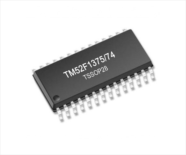
TM52 series F1375/74 are versions of a new, fast 8051 architecture for an 8-bit microcontroller single chip with an instruction set fully compatible with industry standard 8051, and retains most 8051 peripheral’s functional block. Typically, the TM52 executes instructions six times faster than the standard 8051 architecture.
The TM52-F1375/74 provides improved performance, lower cost and fast time-to-market by integrating features on the chip, including 32K Bytes Flash program memory, 1280 Bytes SRAM, Low Voltage Reset (LVR), Low Voltage Detector (LVD), dual clock power saving operation mode, 8051 standard UART and Timer0/1/2, real time clock Timer3, LCD/LED driver, 3 set 16-bit PWMs, 16 channels 12-bit A/D Convertor, 20 channels Touch Key, I2C/SPI interface and Watch Dog Timer. It’s a high reliability and low power consumption feature can be widely applied in consumer and home appliance products.
FEATURES
Standard 8051 Instruction set, fast machine cycle
• Executes instructions six times faster than the standard 8051.
Flash Program Memory
• 32K Bytes (TM52F1375)
• 16K Bytes (TM52F1374)
• Support IAP “In Application Programming” (EEPROM like)
• Code Protection Capability
• 10K erase times at least
• 10 years data retention at least
Total 1280 Bytes SRAM (IRAM + XRAM)
• 256 Bytes IRAM in the 8051 internal data memory area
• 1024 Bytes XRAM in the 8051 external data memory area (accessed by MOVX Instruction)
Four System Clock type selections
• Fast clock from 1~18MHz Crystal (FXT)
• Fast clock from Internal RC (FRC, 18.432 MHz)
• Slow clock from 32768Hz Crystal (SXT)
• Slow clock from Internal RC (SRC,80 KHz)
• System Clock can be divided by 1/2/4/16 option
8051 Standard Timer – Timer0/1/2
• 16-bit Timer0, also supports T0O clock output for Buzzer application
• 16-bit Timer1
• 16-bit Timer2, also supports T2O clock output for Buzzer application
15-bit Timer3
• Clock source is Slow clock
• Interrupt period can be clock divided by 32768/16384/8192/128 option
UARTs
• UART1, 8051 standard UART
• UART2, the second UART, supports only mode1 and mode3
Three independent 16 bits PWMs with period-adjustment
SPI Interface
• Master or Slave mode selectable
• Programmable transmit bit rate
• Serial clock phase and polarity options
• MSB-first or LSB-first selectable
I
2C interface (Master / Slave)
一组主 I2C 接口(Master I2C interface)
20-Channel Touch Key (FTK)
12-bit ADC with 13 channels External Pin Input and 2 channels Internal Reference Voltage
• Internal Reference Voltage: VBG 1.21V @VCC=5V~3V, 25℃
• Internal Reference Voltage: 1/4VCC
LCD Driver
• 1/8 duty
• Software controlled COM0~7
• 1/2 LCD Bias
LED Controller/Driver
• Bidirection matrix mode (BiD) : 4Cx6S, 10 pins up to 48 d
• Dot matrix mode: 8*8, 9 pins up to 64 dots
14 Sources, 4-level priority Interrupt
• Timer0/Timer1/Timer2/Timer3 Interrupt
• INT0~INT1 pin low level or falling edge Interrupt
• INT2~INT9 pin Falling-Edge Interrupt
• Port1 Pin Change Interrupt
• UART1/UART2 TX/RX Interrupt
• ADC/Touch Key Interrupt
• SPI Interrupt
• I
2C interrupt
• PWM0/PWM1/PWM2 interrupt
Pin Interrupt can Wake up CPU from Power-Down (Stop) mode
• INT0~INT9 Interrupt & Wake-up
• Each Port1 pin can be defined as Interrupt & Wake-up pin (by pin change)
Max. 26 Programmable I/O pins
• CMOS Output
• Pseudo-Open-Drain, or Open-Drain Output
• Pin Pull-up can be Enabled or Disabled
• All pin with High sink (60mA@VCC=5V,VOL=0.1VCC)
Independent RC Oscillating Watch Dog Timer
• 400ms/200ms/100ms/50ms selectable WDT timeout options
Five types Reset
• Power on Reset
• Selectable External Pin Reset
• Selectable Watch Dog Reset
• Software Command Reset
• Selectable Low Voltage Reset
16-level Low Voltage Detect
• 4.32V/4.2V/4.08V/3.96V/3.84V/3.72V/3.6V/3.48V/
3.35V/3.23V/3.1V/2.99V/2.86V/2.74V/2.62V/2.52V
8-level Low Voltage Reset
•4.2V/3.96V/3.72V/3.48V/3.23V/2.99V/2.74V/2.52V
Five Power Operation Modes
• Fast/Slow/Idle/Stop/Halt mode
Integrated 16-bit Cyclic Redundancy Check function
Multiplication and division
• 8 bit Multiplier & Divider (standard 8051)
• 16 bits Multiplier & Divider
• 32 bits ÷ 16 bits hardware Divider
On-chip Debug/ICE interface
• Use P3.0/P3.1 pin or P0.0/P0.1 pin
• Share with ICP programming pin
Operating Voltage and Current
• VCC =2.3V ~ 5.5V @FSYSCLK=18.432MHz
• ICC =7µA @Stop mode, VCC=5V
• ICC =1.4µA @Stop mode, VCC=3V
• ICC =150µA @Idle mode, VCC=5V
Operating Temperature Range
• –40°C ~ +85°C
Package Types
• 28-pin SOP28 (300 mil)
• 28-pin QFN32 (4*4*0.75-0.4mm)

